

Plasmonics is an exciting subfield of nanophotonics that explores the interactions between photons and conduction electrons confined near metal/dielectric interfaces. By exploiting these interactions, scientists can manipulate light at subwavelength scales and create strongly enhanced local electromagnetic fields. This can be translated into a broad range of applications, including miniature integrated photonic circuits for communications, optical wavefront engineering, high-efficiency light-emitting and photovoltaic devices, high-resolution imaging and extremely sensitive biosensors.
Plasmon excitation and the associated subwavelength light-matter interaction are extremely sensitive to a variety of physical parameters, making it very attractive for applications in imaging and sensing. The earliest and mostly widely adopted applications of plasmonics are in near-field scanning optical microscopy (NSOM) and surface plasmon resonance (SPR) biosensors. As a collective oscillation of electrons, surface plasmons are wave phenomena that can be focused to tight spots. One can focus a plasmonic field using a highly focused laser beam or the appropriate plasmonic lens structures, such as spatially arranged slits or holes within a thin metal film. The resulting localized plasmonic field may be used as a probe for high spatial resolution imaging, sensing and lithography.
The properties of the optical excitation beams powerfully influence the surface plasmon field. First of all, surface plasmon excitation is strongly dependent on the state of polarization of the incident photons. For example, in the widely used attenuated total reflection configuration, only the p-polarization can excite surface plasmon resonance. The coupling condition also requires the transverse linear momentum of the incident photon and the excited surface plasmon to be matched. This lateral phase-matching condition leads to a very sharp angular resonance. At a fixed incident angle, the dispersion of SPR also causes a sharp resonance in wavelength that can be used for applications in spectral filters.
The polarization sensitivity of SPR excitation raises the interesting possibility that scientists could spatially engineer the state of polarization across the laser beam to match the plasmon coupling condition and achieve optimal plasmonic excitation. The excitation is considered optimal in the sense that it achieves better coupling efficiency from the incident optical beam into plasmon mode and improved focusing in terms of the shape and size of the plasmonic spot. With advances in modern computing and nanofabrication, it is now feasible to manipulate and engineer the state of polarization across the laser-beam profile at the wavelength scale.
We expect scientists to uncover new effects and phenomena that can expand the functionality of optical systems by spatially arranging the local polarization of an optical beam. The so-called cylindrical vector (CV) beams are a special class of these beams with spatially variant polarization. CV beams are the axially symmetric beam solutions to the full vector electromagnetic wave equation. These beams can be generated via different active and passive methods. Radial polarization is a special type of CV beam with its local polarization aligned in the radial direction. Our work explores the matching of optical excitation to the plasmonic structures using radial polarization to achieve optimal plasmonic focusing effects.
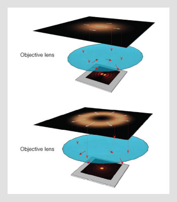 Using radial polarization to achieve optimal plasmonic focusing: (Top) Plasmonic focusing with linear polarization shows the mismatch of symmetry; (Bottom) Symmetry matching achieved with radially polarized optical beam illumination.
Plasmonic focusing on homogeneous metal thin film
A tightly localized plasmonic field can be generated using highly focused laser beams. The beam after a high numerical aperture (NA) contains many angular plane wave components, each of which is associated with a certain incident angle with respect to the surface within the NA. A liquid-immersion objective lens is typically used to satisfy the SPR coupling condition. For those angular plane waves that are p-polarized with respect to the interface and that have the right incident angle to satisfy the phase matching condition, surface plasmons will be excited. These surface plasmon waves propagate and interfere to create a plasmonic focus.
Plasmonic focusing on a uniform metal thin film has been studied with highly focused linear polarization. Due to the depolarization effect of the high NA circular objective, the incident beam is converted into plane waves with different linear polarization states with respect to the interface within a cone of incident angle. Assuming the incident polarization is in the tangential plane of the objective lens, for plane wave components that are in the tangential plane, the state of polarization is purely p-polarized with respect to the surface, while those plane wave components in the sagittal plane will be purely s-polarized.
For plane waves in-between the tangential and sagittal planes, the state of polarization will be a combination of s- and p-polarized. Due to polarization selectivity, only those plane waves with a p-polarized component could be coupled into surface plasmons. Thus, using linear polarization with a high-NA circular objective lens creates a mismatch for the plasmon excitation condition. The plasmonic focus generated this way is inhomogenous, and the coupling from the optical field into the plasmonic field is inefficient. Even worse, the plasmonic waves generated by the plane waves from the opposite side of the objective lens are out of phase at the geometric center, leading to a splitted plasmonic field with a dip in the middle.
A laser beam with radial polarization can be used to match the optical illumination to the surface plasmon generation condition for optimal focusing effect. Radial polarization is a spatially variant polarization with a vector singularity point at the beam center, and the local polarization is aligned along the radial direction. Unlike with linearly polarized beams, when a radially polarized beam is focused onto an axially symmetric plasmonic structure, the entire beam is p-polarized with respect to the interface, enabling surface plasmon excitation from all directions. In addition, a homogeneous plasmonic focal spot can be obtained through the constructive interference of these plasmon waves.
We have experimentally verified such an optimal plasmonic focusing effect using a sample with a 50-nm silver layer deposited on a glass substrate. The plasmonic focus generated this way is an evanescent field that decays from the metal/dielectric interface. More interestingly, due to the angular selectivity of the SPR and the axial symmetry of the setup, only the incident angular plane waves within a narrow cone of angles will be coupled to the SPR. Such an angular selectivity mimics the function of the classical axicon. Consequently, the plasmonic focus generated this way is an evanescent “non-spreading” Bessel beam. The combination of radial excitation symmetry, and the SPR angular selectivity, eliminates the need for an axicon and significantly simplifies the alignment procedure.
With a radially polarized 532-nm laser beam, we have observed through NSOM scanning a plasmonic evanescent Bessel field with a spot size of 195 nm and decay length of 143 nm. Combined with the field enhancement effect associated with SPR, this type of evanescent focal field can interact more efficiently with samples near the surface, leading to a higher signal-to-noise ratio and shorter detection time—both of which are critical for many imaging or sensing applications.
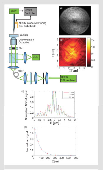 Near-field optical imaging verification of the plasmonic focusing under radial polarization illumination: (a) SPR resonance on a silver film; (b) NSOM image of the focusing plasmonic waves; (c) Normalized transverse profiles of the NSOM signals at different distances from the sample surface. All curves almost overlap, indicating the non-spreading property of the field. (d) The measured evanescent decay of the plasmonic focus field away from the surface.
Plasmonic focusing with concentric rings
In the example we just described, plasmonic focusing was realized with the help of a high-NA optical objective lens, which is used to provide the phase matching for plasmon coupling. The same plasmonic focusing effect can be achieved with a flat plasmonic lens, which can be fabricated with spatially arranged subwavelength metal structures, such as notches, holes and slits in a metal thin film.
For example, X. Zhang et al. have demonstrated focusing with a circular slit. The scattering from these subwavelength structures provide the necessary coupling from optical energy into plasmonic waves. By making a circular subwavelength slit into a silver film, the plasmon waves excited at the edges of the slit will have a curved wavefront and be focused toward the geometrical center. However, again due to the mismatch between the polarization of the excitation beam and the plasmonic structure, only part of the beam is p-polarized with respect to the flat plasmonic lens, and the focus generated this way is inhomogeneous. In addition, if the incident beam is aligned with the center of the circular plasmonic lens, the plasmon waves generated at the opposite side of the circular slit will have opposite phase and destructively interfere, creating a dip rather than a strong peak in the center.
We have demonstrated that radial polarization can also be used to improve the excitation and focusing of these flat plasmonic lenses. From numerical simulations, plasmonic focusing is clearly observed for a single circular slit carved into a metal thin film as well as plasmonic lens structures that consist of multiple concentric rings (bull’s eyes). In the latter case, if the location and the rings are chosen to satisfy the circular Bragg condition for the plasmonic wavelength, the peak intensity of the plasmonic center will become stronger as more rings are added to the lens structure, while the focal spot remains approximately the same size.
As shown in the numerical simulation, the electrical field distribution inside the metal film clearly confirms the electron density oscillation at the metal/dielectric interface. There are several other interesting properties to note. The electric field near the vicinity of the focus is purely polarized along the longitudinal direction normal to the interface, generating a kind of optical “needle” field similar to that reported recently by researchers who used a combination of multiple zone diffractive optical elements and a high-NA objective lens. The bull’s eye flat plasmonic lens provides a more compact and simpler alternative. In addition, on both sides of the plasmonic lens, the vector electric field shows polarization vortex structures near the slits that are worthy of further investigation.
We also conducted experiments to verify the focusing effect with the Bull’s eye plasmonic lens. First, we fabricated multiple concentric rings with focus ion beams in 200-nm-thick silver film deposited on glass. The width of the rings is also 200 nm. Then, we aligned a 532-nm slightly focused radially polarized laser beam with the center of the Bull’s eye. NSOM images reveal that, indeed, the plasmonic waves are generated from all directions and focus toward the center. We are in the process of comparing the focusing effect with a different number of rings to determine the field enhancement effect qualitatively.
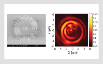 Plasmonic lens structures that consist of multiple concentric rings: (Left) SEM image of a 9-ring bull’s eye plasmonic lens in silver film; (Right) NSOM imaging shows the focusing of the plasmonic lens under radial polarization.
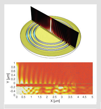 Electrical field distribution inside the metal film: (Top) Illustration of a plasmonic lens with three concentric rings etched into a 200-nm silver film on glass with a slice of the computed plasmonic field; (Bottom) Details of the computed electric field and the electric vector distribution. Polarization vortex structures can be clearly identified.
Plasmonic focusing on particles and conical antennas
Besides the planar metal/dielectric interface and the nanostructured flat plasmonic lens, other axially symmetric plasmonic structures—including metallic coated conical antenna and spherical, ellipsoidal or cylindrical metallic nanoparticles—will also benefit from using radially polarized illumination. For example, focused radial polarization can be used to tailor SPR excitation on spherical silver nanoparticles and offer more opportunities than conventionally polarized light beams. This interesting finding could lead to applications in optical spectroscopy using metal nanoparticles, optical tweezers and optical data storage.
We have studied the plasmonic focusing with a conical antenna under the internal illumination of radial polarization. The conical antenna is made of a dielectric sharp tip that is fully coated with metal. When radial polarization is launched into the dielectric conical tip, the entire beam is p-polarized with respect to the dielectric/metal interface. Due to diffraction, the mode field pushes out as it propagates toward the tip apex and consequently excites the surface plasmon along the dielectric/metal interfaces. Surface plasmons excited by the p-polarized light, which propagates toward the end of the tip and interferes constructively due to the rotational symmetry of both the structural geometry and the polarization state of illumination. This creates a strongly localized and enhanced field at the tip apex.
From the numerical simulations, we found that, at the optimized cone angle, an intensity enhancement factor as high as 10,000 (corresponding to a field enhancement of 320) can be achieved with a sharp glass cone that is completely coated with a 50-nm silver film. The intensity enhancement has strong dependence on the shape of the tip. The strong field enhancement effect is associated with a tight spatial confinement of a few tens of nanometers for the plasmonic field. With 632.8 nm excitation, a full-width-half-maximum plasmonic spot size as small as 10 nm is possible. Such a strong localization and high field enhancement make this type of plasmonic antenna very attractive for near-field optical imaging applications.
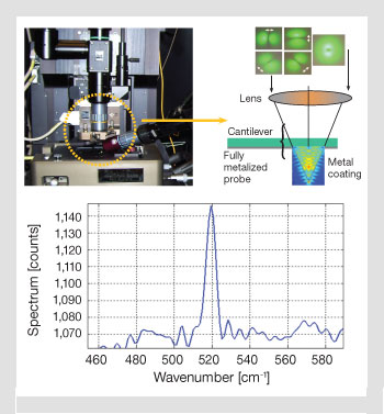 Electrical field distribution inside the metal film: (Top left) The vertical column is used for illumination, and the objective lens on the side is for Raman signal collection. (Top right) Details of the illumination and the cantilever probe with the electrical field simulated by COMSOL superimposed. (Bottom) A near-field Raman spectrum of 520 cm-1 for silicon using a silver-coated conical glass tip.
Future directions
Optimal plasmonic focusing offers tremendous advantages in terms of the plasmonic focus shape, peak intensity and spatial localization. It may find applications in more efficient coupling for plasmonic circuits, local electromagnetic field concentration, high-resolution imaging, biochemical sensing and thin film characterization. For example, researchers have recently used the evanescent Bessel beam generated with plasmonic focusing on homogeneous metal film in the imaging of cell-substrate interface of a biological cell in aqueous media. The local field enhancement at the apex of the conical plasmonic antenna may find important near-field scanning optical microscopy applications such as near-field Raman, fluorescence, two photon absorption, second harmonic generation, etc.
One application that we find particularly interesting is in semiconductor metrology. Progress in nanofabrication and nanotechnology continuously drive semiconductor devices toward becoming smaller, faster, cheaper and more complex. As an integral part of semiconductor manufacturing, metrology tools are indispensable in yield improvement and cost reduction. As the semiconductor industry moves toward silicon nanoelectronics, the introduction of new fabrication processes, new materials and novel devices bring formidable challenges to current metrology tools.
For example, in some recently introduced strained silicon structures, a layer of gradient SiGe is first built upon a bulk silicon substrate; then, a thin layer of silicon is deposited on the relaxed SiGe layer. Due to lattice mismatch, strain is created in the deposited Si layer that can lead to higher electron mobility for faster devices. Metrology of the strain/stress in the strained silicon substrate as well as the Si channel of fabricated devices is crucial for determining the lattice strain that affects the electronic band structure to provide mobility enhancement. In addition, residual strain/stress in devices after fabrication affects their long-term reliability—which also underscores the need for stress/strain metrology solutions at the device level.
Raman spectroscopy is one of the leading candidates to meet this metrology challenge. It requires minimal sample preparation, and stress/strain metrology is possible due to the Si-Si Raman shift dependence on the stress level. However, collecting a reliable Raman signal from a spatial dimension less than 50 nm within reasonable integration time is a daunting challenge due to the extremely low scattering cross-section of the Raman process.
Currently, we are implementing a near-field Raman mapping system that uses the conical plasmonic antenna under radial polarization internal illumination. The field enhancement effect provided by the plasmonic focusing at the tip apex increases the signal level while the internal coupling eliminates background noise. We have observed an intensity enhancement of 900, with integration time reduced from 300 to 1 s. We are working on verifying our results and plan to publish them in the near future.
The authors would like to acknowledge the financial supports and collaborations from AFRL, AFOSR, ODOD, DAGSI, University of Dayton School of Engineering, IDCAST, IZFP-Dresden and HSEB GmbH.
Qiwen Zhan and Weibin Chen are with the electro-optics graduate program at the University of Dayton in Dayton, Ohio, U.S.A. Robert L. Nelson is with the Air Force Research Laboratory at Wright-Patterson Air Force Base in Dayton, Ohio, U.S.A. Don C. Abeysinghe is with the department of electrical and computer engineering at the University of Cincinnati, Cincinnati, Ohio, U.S.A.
References and Resources
>> H. Kano et al. J. Opt. Soc. Am. B. 15, 1381 (1998).
>> Z. Liu et al. Nano Letters 5, 1726 (2005).
>> L. Yin et al. Nano Letters, 5, 1399 (2005).
>> Q. Zhan. Opt. Lett. 31, 1726 (2006).
>> A. Bouhelier et al. Opt. Lett. 32, 2535 (2007).
>> W. Chen and Q. Zhan. Opt. Express 15, 4106 (2007).
>> W. Chen and Q. Zhan. Chin. Opt. Lett. 5, 709 (2007).
>> W. Chen and Q. Zhan. Proc. SPIE 6450, 64500D (2007).
>> K.J. Moh et al. Opt. Express 16, 20734 (2008).
>> H.F. Wang et al. Nature Photon. 2, 501 (2008).
>> Q. Zhan. Adv. Opt. Photon. 1, 1 (2009).
>> W. Chen and Q. Zhan. Opt. Lett. 34, 722 (2009).
>> A. Yanai and U. Levy. Opt. Express 17, 924 (2009).
>> N.M. Mojarad and M. Agio. Opt. Express 17, 117 (2009).
>> K.J. Moh et al. Opt. Lett. 34, 971 (2009).